Si3N4 DBC and AMB ceramic substrates
With the development of wide bandwidth semiconductors, power semiconductor devices to higher power density, higher chip temperature and higher reliability of the direction of development, and accordingly for the power semiconductor module packaging put forward higher requirements. Including our previous talk about no solder, no bonding wires and other interconnect technology trends, the choice of insulation substrate has also become a frequent topic of discussion.
In order to improve the thermal performance of the module, it is necessary to place an insulating substrate with high thermal conductivity between the chip and the backplane. The main method of constructing circuit interconnects on insulating substrates is DBC (Direct Bonded Copper), in which a ceramic insulating layer – with very good electrical insulation and dielectric strength – is bonded directly between two layers of copper. These substrates are usually selected based on the application and their thermal, mechanical and electrical insulation properties.
Earlier we also had a brief chat about insulating substrates
Power Module I – Insulated Substrate and Power Module II – Insulated Substrate Metallisation
Common insulating substrate materials include alumina (Al2O3 and HPS doped with 9% zirconia), aluminium nitride (AlN), silicon nitride (Si3N4), etc. Among them, Al2O3 is the most economical. Al2O3 is considered the most economical choice, although it has relatively high mechanical strength, but compared with other materials, thermal conductivity appears to be a lot weaker, relatively less suitable for the development of subsequent power devices; AlN has a higher thermal conductivity, CTE and silicon is almost the same, effectively reducing the delamination and solder fatigue and other issues, but the mechanical strength of the thermal cycle in a larger is not enough to have the advantage. Si3N4 CTE is also very close to the semiconductor chip, while providing good mechanical strength and thermal fatigue, but the cost and supply is relatively speaking a “weak point”, but now we are in the high-performance module is still very common, the use of silicon nitride substrate in the future should become more common.
A friend recently shared a Rogers article on the comparison of Silicon Nitride DBCs and AMBs.
‘Comparison of Silicon Nitride DBC and AMB Substrates for different applications in power electronics’
Based on this, let’s talk a little more about insulating substrates.
Silicon Nitride DBC and AMB
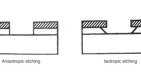
DBC (Direct Bonded Copper) and AMB (Activated Metal Brazing) technologies are the two most common copper laying processes for substrates today, and below is a simple diagram of the two manufacturing processes.
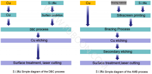
The basic principle of DBC is to introduce oxygen between the copper and the ceramic substrate to form a Cu/O eutectic liquid phase at about 1000°C, which in turn adheres to the ceramic substrate. However, AlN and Si3N4, for example, require a layer of oxidation on their surfaces first before the conventional DBC process can be satisfied.
The basic principle of AMB is that the solder containing the active elements Ti and Zr is wetted and reacted at the interface between ceramic and metal at a temperature of 900°C, resulting in bonding.
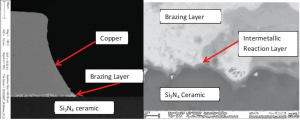
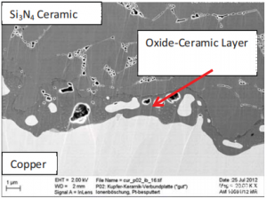
The SEM electron microscope scanning interface image shown above allows us to see each layer more clearly.
Si3N4 Ceramic Substrate Characteristics
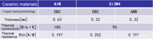
And we can see that other things being equal, the thermal resistance of Si3N4 with DBC and AMB is also almost the same.
Thermal Shock
In order to understand the reliability of several different ceramic substrates, they are characterised and compared by thermal shock testing, below are the comparisons of AlN, Al2O3, HPS, Si3N4 (DBC & AMB).
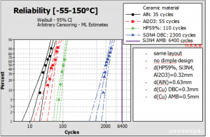
We can see that under the same conditions, the Si3N4 DBC substrate is 20 times more resistant to thermal shock than the common Al2O3 DBC substrate, and its AMB substrate (0.5mm copper layer) is more than 50 times more resistant.
Electrical insulation performance
Several ceramic substrates were tested for partial discharge and breakdown strength under the following conditions: 50Hz AC at the ball electrode, 1kV/s change rate, measuring partial discharge at 5kV and increasing the voltage until breakdown occurs. The test results are as follows.
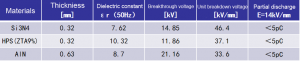
The electrical insulation properties of all ceramic substrates are pretty good, so we generally don’t talk too much about the implications of this.
Layout recommendations
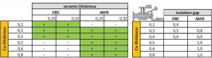
Si3N4 DBC and AMB ceramic substrates
The insulation gap of AMB ceramic substrates must be slightly larger than that of DBC’s, and the necessary etching process to remove the brazing material limits the minimum size in this regard. The need for high power densities means higher currents, and AMB allows for thicker copper layers (0.3mm to 0.8mm), i.e. the ability to have higher current carrying capacity.
Below is a map of the application areas related to isolation voltage and thermal conductivity of ceramic substrates given in the article
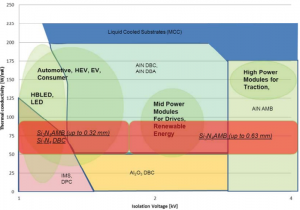
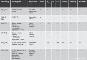
As well as the advantages and disadvantages of the characteristics of different ceramic substrates and the corresponding comparison of the relevant applications.
Summary
The content focuses on understanding the properties of Si3N4 DBC and AMB ceramic substrates and comparing them to several major ceramic substrates. As with everything, there is basically one key factor that comes into play, “cost”, and more often than not we see traditional Al2O3 DBC substrates or HPS substrates doped with 9% zirconia for increased mechanical strength. Si3N4 DBC or AMB substrates can only be found in areas where there is a trade-off between better performance and cost.
Si3N4 DBC and AMB ceramic substrates