Semiconductor Processes – Etching
1, etching process classification:
There are two main types of etching processes in semiconductor manufacturing: dry etching and wet etching. Dry etching is divided into three: plasma etching, ion beam sputtering etching and reactive ion etching (RIE). Of course, etching can also be divided into graphic etching and graphic etching. Patterned etching using photoresist or other materials as a mask, only the bare part of the etching off, while no patterned etching is carried out in the absence of a mask.
2, the purpose and problems of etching:
In the graphic transfer or replication of the accuracy relies on several process parameters: incomplete etching, over-etching (overetch), drilling etching, selecting the ratio and the side of the various anisotropic / various isotropic etching.
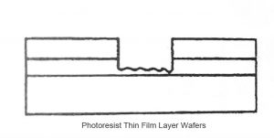
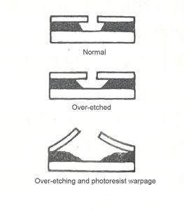
Incomplete etching: The reasons may be, firstly, that the etching time is too short and, secondly, that the thickness of the film to be etched is not uniform.
Over-etching: In any etching process, there will always be a degree of planned over-etching to allow for variations in the thickness of the surface layer, or for the next step in the process.
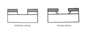
Isotropic and Anisotropic: Isotropic means that the etching will be done in all directions; anisotropic is the opposite, so anisotropy will give a better etching pattern (vertical sides) than isotropy.
Drill Etching: The process of etching starting from the outermost surface to the bottom also takes place on the outermost surface and results in the formation of a bevelled surface on the side. When this action is etched under the photoresist edge, it can be called drill etching.
Semiconductor Processes – Etching
Selection ratio: refers to the same etching conditions in two different materials etching rate faster than the ratio. For example: when the photoresist as a mask needs to be etched SIO2, with dry etching, then you need to consider the etching in the same time, photoresist and SIO2 etching ratio. Otherwise there will be photoresist as a mask has been etched out, SIO2 has not been etched to the required requirements.
Uniformity: is a measure of the etching process on the entire wafer, or the entire batch, or batch to batch etching ability of the parameter. Uniformity is closely related to the selection ratio because non-uniform etching produces additional over-etching. Some of the problems with uniformity arise as a result of the etch rate and etch profile as it relates to the size and density of the pattern. The etch rate is slower in small-window patterns, and the etching can even stop on small-size patterns with high aspect ratios, a phenomenon known as aspect-ratio dependent etching (ARDE), also known as the microloading effect. To improve uniformity, the ARDE effect on the wafer surface must be minimised.
In addition to the above parameters, residues, polymers, plasma-induced damage, and particle staining are also parameters of the etching technique in actual production.
3, Summary:
Wet etching: wet spray etching, immersion etching.
Advantages: lower cost, can be batch, etc..
Disadvantages: 1, limited to more than 2um graphic size; 2, isotropic, will be lateral corrosion leads to the formation of a certain slope on the side; 3, in the wet etching must be required after rinsing and drying steps; 4, a variety of corrosive agents are toxic as well as potentially contaminated; 5, the failure of the adhesive capacity of the photoresist leading to the drilling of corrosion.
Dry etching: plasma, ion milling and reactive ion etching (RIE)
Advantages: good selection ratio, can achieve smaller graphic size, can accurately control the accuracy and so on.
Disadvantages: slow and expensive.
Semiconductor Processes – Etching