ўВЎЈЎє ЎІўДўДўКЎ≤Ў± ЎІўДЎ±ўГўКЎ≤Ў© ЎІўДЎ≥ўКЎ±ЎІўЕўКўГ ЎІўДЎ£ўДўИўЕўКўЖЎІ
- ўИЎµўБ
- Ў≥Ў§ЎІўД
ўВЎЈЎє ЎІўДўДўКЎ≤Ў± ЎІўДЎ±ўГўКЎ≤Ў© ЎІўДЎ≥ўКЎ±ЎІўЕўКўГ ЎІўДЎ£ўДўИўЕўКўЖЎІ
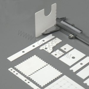
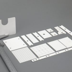
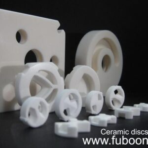
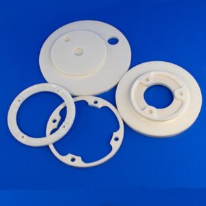
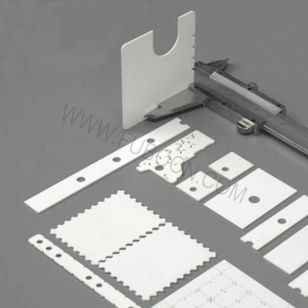
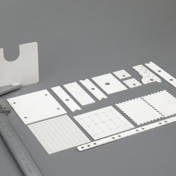
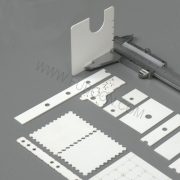
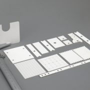
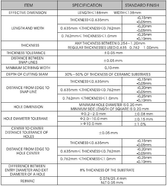
The high precision laser cutting processing installations can be used for scribing, cutting and drilling ceramic substrates (Minimum hole diameter:0.2ўЕўЕ).Laser cutting method allows to produce ceramic substrates with
various outside contour geometries, hole patterns, cut-outs and snap-lines.
Benefits:
вЧПHigh cutting accuracy, very small tolerance.
вЧПEliminating the time-consuming and costly tool fabrication stage.
вЧПAs well as increasing the goods supply efficiency by a big margin and shortening the processing circle.
CRITERIA OF SUBSTRATES BY LASER PROCESS
ўВЎЈЎє ЎІўДўДўКЎ≤Ў± ЎІўДЎ±ўГўКЎ≤Ў© ЎІўДЎ≥ўКЎ±ЎІўЕўКўГ ЎІўДЎ£ўДўИўЕўКўЖЎІ
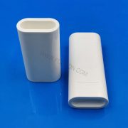
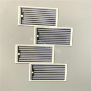
Ceramic substrate refers to a special process board in which copper foil is directly bonded to the surface of alumina (Al2O3) or aluminum nitride (AlN) ceramic substrate (single or double) at high temperature. The made of ultra-thin composite substrate with excellent electrical insulation properties, ЎІўДўЕўИЎµўДўКЎ© ЎІўДЎ≠Ў±ЎІЎ±ўКЎ© ЎІўДЎєЎІўДўКЎ©, excellent solderability and high adhesion strength, and the same as the PCB can be etched a variety of graphics, with a large current carrying ability. ўДЎ∞ўДўГ, the ceramic substrate has become the basis of high-power power electronic circuit structure technology and interconnect technology.
ўДўИўКЎ≤ўКЎІўЖЎІ Ў®ўКўДўКўЗ ЎђЎ±ўКўД ЎІўДЎіЎІЎєўД:
1. High Power Power Semiconductor Modules; Semiconductor Coolers, Electronic Heaters; Power Control Circuits, Power Hybrid Circuits.
2. Smart Power Components; High Frequency Switching Power Supply, Solid State Relays.
3. ЎІўДЎ≥ўКЎІЎ±ЎІЎ™, Aerospace and Military Electronics Components.
4.Solar panel components; telecommunications switches, receiving systems; lasers and other industrial electronics.
ўВЎЈЎє ЎІўДўДўКЎ≤Ў± ЎІўДЎ±ўГўКЎ≤Ў© ЎІўДЎ≥ўКЎ±ЎІўЕўКўГ ЎІўДЎ£ўДўИўЕўКўЖЎІ
Superiority:
1. Ceramic substrate thermal expansion coefficient close to the silicon chip can save the transition layer Mo film, saving labor, ЎІўДўЕўИЎІЎѓ, reduce costs;
2. Reduce solder layer, lower thermal resistance, reduce voids, improve yield;
3. The 0.3mm-thick copper foil at the same current carrying capacity is only 10% of the normal printed circuit board;
4. ЎІўДўЕўИЎµўДўКЎ© ЎІўДЎ≠Ў±ЎІЎ±ўКЎ© ЎІўДўЕўЕЎ™ЎІЎ≤Ў©, the chip package is very compact, so that the power density greatly improved and improve system and device reliability;
5. Ultra-thin (0.25ўЕўЕ) ceramic substrate can replace BeO, no environmental toxicity issues;
6. Current carrying capacity, 100A continuous current through the 1mm wide and 0.3mm thick copper body, the temperature rise of about 17 Ў£ўЕЎІўЗ ўБўК ЎЄўД ЎЄЎ±ўИўБ ЎІўДЎєўЕўД ЎІўДЎєЎІЎѓўКЎ©; 100A current through a continuous 2mm wide and 0.3mm thick copper Body, temperature rise is only about 5 Ў£ўЕЎІўЗ ўБўК ЎЄўД ЎЄЎ±ўИўБ ЎІўДЎєўЕўД ЎІўДЎєЎІЎѓўКЎ©;
7. Low Thermal Resistance, Thermal Resistance of 10 √Ч 10mm Ceramic Substrate 0.63mm Thickness Thermal Resistance of Ceramic Substrate 0.31K / ЎѓЎ®ўДўКўИ, 0.38mm Thickness Heat of Ceramic Substrate
8. Resistance is 0.19K / ЎѓЎ®ўДўКўИ, 0.25mm thickness of the thermal resistance of the ceramic substrate is 0.14K / ЎѓЎ®ўДўКўИ. High dielectric strength, personal safety and equipment protection.
9. Allows for new packaging and assembly methods that make the product highly integrated and compact.
ўЕўЖЎ™ЎђЎІЎ™ Ў∞ЎІЎ™ ЎµўДўЗ
Ў£ЎђЎ≤ЎІЎ° ўВЎ±Ўµ ЎµўЕЎІўЕ Ў≥ўКЎ±ЎІўЕўКўГ ЎІўДЎ£ўДўИўЕўКўЖЎІ
ўВЎ±Ўµ Ў≥ўКЎ±ЎІўЕўКўГ Ў£ўДўИўЖўКўЕЎІ ўДЎЃЎ±ЎЈўИЎіЎ© ўИЎµўЕЎІўЕ ЎІўДЎ≠ўЖўБўКЎ© .
ЎІўДЎ£ўДўИўЕўКўЖЎІ Ў®ЎЈЎІўЖЎ© Ў£ўЖЎ®ўИЎ® ўГўЕ ЎІЎ≥ЎЈўИЎІўЖЎ© ўДўДўЕЎґЎЃЎ©
Ў£ўЖЎ®ўИЎ® Ў®ЎЈЎІўЖЎ© ЎІўДЎ£ўДўИўЕўКўЖЎІ / ЎђўДЎ®Ў© / Ў£Ў≥ЎЈўИЎІўЖЎ© ўДўДўЕЎґЎЃЎ©
ўЕўГўИўЖЎІЎ™ Ў≥ўКЎ±ЎІўЕўКўГ ЎІўДЎ£ўДўИўЕўКўЖЎІ
ўЕўГўИўЖЎІЎ™ Ў≥ўКЎ±ЎІўЕўКўГ ЎІўДЎ£ўДўИўЕўКўЖЎІ
ўБЎ±ўЖ ЎІўДўБЎ±ўЖ Ў£ўЖЎ®ўИЎ® Ў≥ўКЎ±ЎІўЕўКўГ ЎІўДЎ£ўДўИўЕўКўЖЎІ ЎІўДўЕўВЎІўИўЕ ўДЎѓЎ±ЎђЎІЎ™ ЎІўДЎ≠Ў±ЎІЎ±Ў© ЎІўДЎєЎІўДўКЎ©
Ў£ўЖЎ®ўИЎ® Ў≥ўКЎ±ЎІўЕўКўГ ЎІўДЎ£ўДўИўЕўКўЖЎІ ЎєЎІўДўК ЎІўДЎ≠Ў±ЎІЎ±Ў©
ўВЎґўКЎ® Ў≥ўКЎ±ЎІўЕўКўГ ўЕўЖ ЎІўДЎ£ўДўИўЕўКўЖЎІ ЎІўДўЕўВЎІўИўЕ
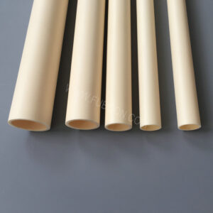
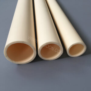
ўВЎґўКЎ® Ў≥ўКЎ±ЎІўЕўКўГ ўЕўЖ ЎІўДЎ£ўДўИўЕўКўЖЎІ ЎІўДўЕўВЎІўИўЕ 3 ўЕўЕ – 25ўЕўЕ
Ў£ўЖЎІЎ®ўКЎ® ЎђўДЎ®Ў© ЎђўДЎ®Ў© Ў≥ўКЎ±ЎІўЕўКўГ ЎІўДЎ£ўДўИўЕўКўЖЎІ
ўЕЎє ўЕўВЎІўИўЕЎ© ЎІўДЎ™ЎҐўГўД hign ўИўЕўВЎІўИўЕЎ© ЎІўДЎ™ЎҐўГўД ЎІўДўЕўДЎІЎ¶ўЕЎ©,ўКЎ≥Ў™ЎЃЎѓўЕ Ў£ўЖЎ®ўИЎ® ЎІўДЎ≥ўКЎ±ЎІўЕўКўГ ЎєўДўЙ ўЖЎЈЎІўВ ўИЎІЎ≥Ўє ўБўК Ў®ўКЎ¶Ў© ЎєЎІўДўКЎ© ЎІўДЎ™ЎҐўГўД ўИЎєЎІўДўКЎ© ЎІўДЎ≠Ў±ЎІЎ±Ў© ўЕЎЂўД ўЕЎ≠ЎЈЎІЎ™ ЎІўДЎЈЎІўВЎ© ЎІўДЎ≠Ў±ЎІЎ±ўКЎ©,ЎІўДЎ™ЎєЎѓўКўЖ,ЎєўДўЕ ЎІўДўЕЎєЎІЎѓўЖ,ўЕЎµЎІўЖЎє ЎІўДЎІЎ≥ўЕўЖЎ™,Ў•ўДЎЃ.
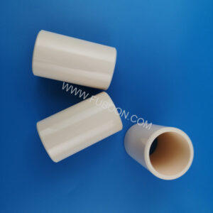
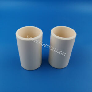
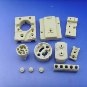
ўБўИўЗЎ© Ў≥ўКЎ±ЎІўЕўКўГ ЎІўДЎ£ўДўИўЕўКўЖЎІ ЎІўДЎµўЖЎІЎєўКЎ©
ўБўИўЗЎ© Ў≥ўКЎ±ЎІўЕўКўГ ўДўДЎ≠ЎІўЕ ўИўЖЎ≥ўБ ЎІўДЎ±ўЕЎІўД
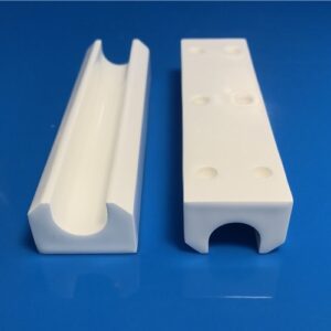
ЎєўИЎІЎ≤ўД Ў≥ўКЎ±ЎІўЕўКўГ ўГўЗЎ±Ў®ЎІЎ¶ўКЎ©
ЎєўИЎІЎ≤ўД Ў≥ўКЎ±ЎІўЕўКўГ ўДўДЎ≥ЎЃЎІўЖЎІЎ™ ЎєўИЎІЎ≤ўД Ў≥ўКЎ±ЎІўЕўКўГ ўГўЗЎ±Ў®ЎІЎ¶ўКЎ©
ЎєЎІўГЎ≥ ўДўКЎ≤Ў± Ў≥ўКЎ±ЎІўЕўКўГ ЎІўДЎ£ўДўИўЕўКўЖЎІ
ЎєЎІўГЎ≥ ўДўКЎ≤Ў± Ў≥ўКЎ±ЎІўЕўКўГ ЎІўДЎ£ўДўИўЕўКўЖЎІ
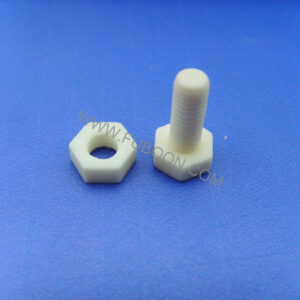
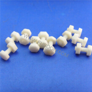
Ў®Ў±ЎЇўК Ў≥ўКЎ±ЎІўЕўКўГ ЎІўДЎ£ўДўИўЕўКўЖЎІ
M2 M3 M4 M5 M6 Ў®Ў±ЎЇўК Ў≥ўКЎ±ЎІўЕўКўГ ЎІўДЎ£ўДўИўЕўКўЖЎІ / ЎµўЕўИўДЎ© Ў≥ўКЎ±ЎІўЕўКўГ